Micron G11 NAND: 400+ layers and double density in 2027
Micron skips G10 and announces G11 3D NAND with over 400 layers, about twice G9's bit density and up to 50% faster I/O. Volume production starts in late 2027.
LandGadget Newsroom · · 3 min read
On this page
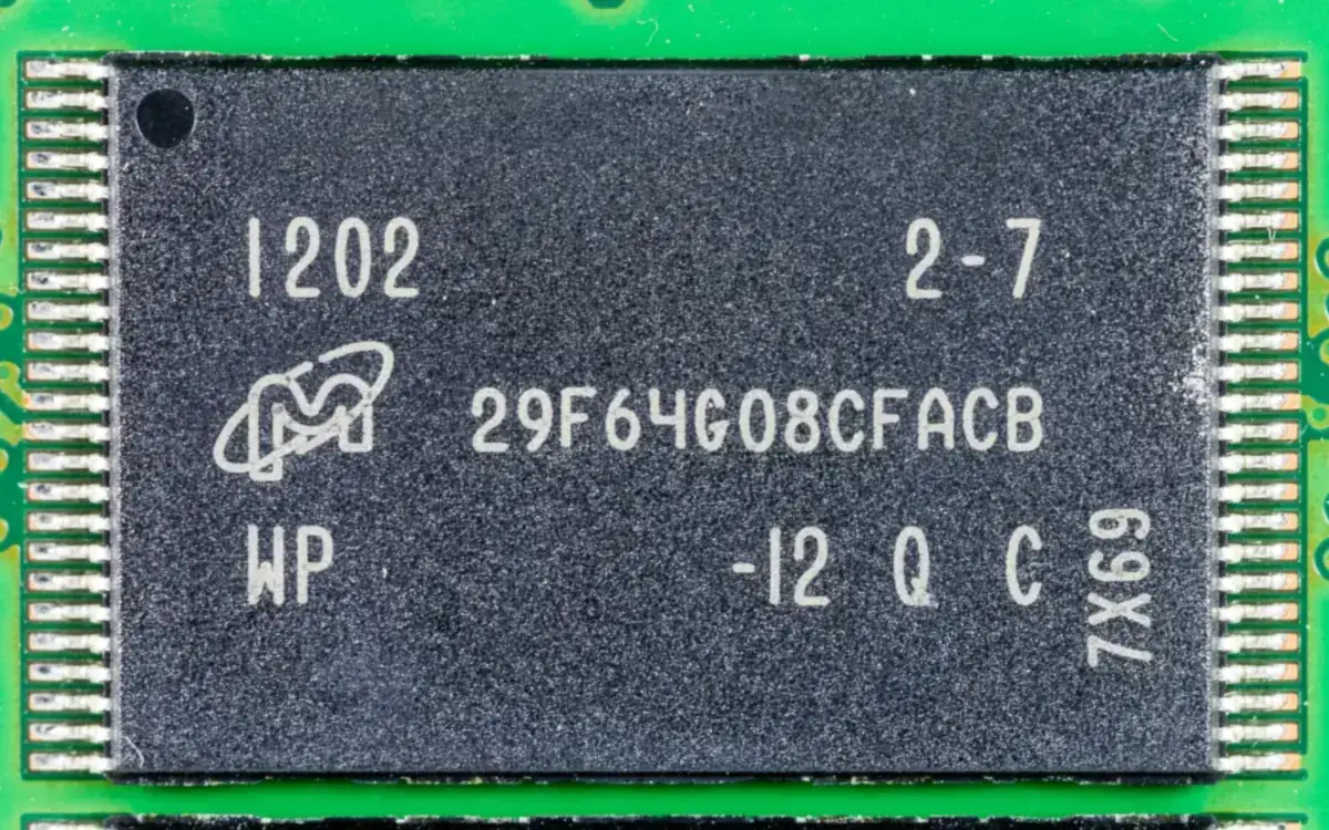
Micron has shown its next big step in flash memory, and it has skipped a number to get there. At a technology webinar this week the company announced G11 3D NAND, going straight from today's G9 to G11, Tom's Hardware reports. Skipping a generation name isn't unusual in the memory business, but the specs suggest a real leap.
What Micron promises
- More than 400 layers, up from 276 in G9 (used in drives such as the Crucial P510). Micron hasn't said exactly how many active layers or decks there are.
- About twice the bit density of G9, thanks to the extra layers plus what Micron calls an "industry-leading" cell pitch.
- Up to 50% faster I/O. Tom's Hardware works that out as roughly 3,600 → 5,400 MT/s, but that is the outlet's calculation, not a figure Micron has published.
- More than 25% lower energy per bit transferred.
Some outlets quote a density of 42 Gb/mm². That number is an estimate made by doubling a previously cited G9 figure, and it isn't confirmed by Micron. It's also unclear whether the comparison is for TLC (3 bits per cell) or QLC (4 bits) chips, which makes a big difference.
The key change: wafer bonding
G11 uses wafer-on-wafer bonding. Micron builds the memory array on one wafer with a new 3D NAND process and the peripheral logic and I/O circuits on a separate wafer with a logic process, then bonds the two together. China's YMTC already uses a similar approach. Micron's previous generations put the logic under the memory array on the same wafer.
"We had mentioned we will bring in wafer-on-wafer bonding technology at the right time when it's cost-effective," said Scott DeBoer, Micron's president and chief technology and products officer, calling G11 "the world's most advanced NAND."
Beyond G11, Micron is working on high-mobility materials and ultra-dense cell architectures, so future gains come from shrinking cells as well as stacking more layers. It hasn't given dates for those.
When you'll see it
Not soon. Volume production starts in the second half of 2027, and Micron plans to share more technical detail closer to then. Consumer SSDs normally follow a new NAND generation by some months, and the first buyers are usually data centres, where AI workloads are driving demand for dense, fast storage.
What it means for buyers
Denser NAND is how SSDs get bigger and, over time, cheaper per terabyte, but memory prices also depend on supply and AI demand, as the debate over PS6 memory costs shows. If you need a drive today, our SSD buying guide explains what actually matters, and fast external enclosures like Ugreen's 20Gbps M.2 case can give an older drive a second life.
More from Computers & AI
View all →Read next

NASA's new Artemis plan: Earth-orbit test, landing in 2028
Artemis III becomes a 2027 Earth-orbit test with both commercial landers, and the first crewed landing moves to 2028 with whichever lander is ready first.

Steam Personal Calendar leaves Labs: release dates for you
Steam's Personal Calendar is now a full feature: an 8-week list of upcoming releases picked from your playtime, with wishlist, DLC and Early Access filters.
How to check battery health on iPhone and Android
How to check your phone's battery health on iPhone, Samsung Galaxy, Pixel and other Android phones, what the numbers mean, and when a battery replacement is worth it.